Skip to content
marcorhyoe.digiblogbox.com
Welcome to our Blog!
No posts yet
1
2
3
4
5
6
7
8
9
10
11
12
13
14
15
Celebrity Then and Now
Anna Chlumsky Then & Now!
Molly Ringwald Then & Now!
Bug Hall Then & Now!
James Van Der Beek Then & Now!
Matilda Ledger Then & Now!
Search for:
Links
Log in
Homepage
Start page
Start your own blog
Start your own blog
Report this page
Archives
2025
Categories
Blog
Meta
Log in
Entries
RSS
Comments
RSS
WordPress.org
1
2
3
4
5
forum
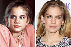 Anna Chlumsky Then & Now!
 Molly Ringwald Then & Now!
 Bug Hall Then & Now!
 James Van Der Beek Then & Now!
 Matilda Ledger Then & Now!